Industry-Specific Laser MicroJet Benefits
Synova’s unique water jet guided laser systems offer many advantages for applications in the semiconductor industry compared to conventional diamond blade saws or laser systems.
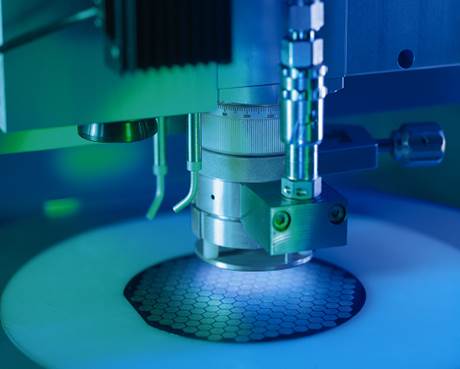
The “gentle” Laser MicroJet (LMJ) method enables the cutting, grooving and dicing of sensitive materials resulting in smooth edges, high wafer fracture strength and less risk of breakage. The flexible LMJ technology allows precise ablation of various semi-conductor materials such as silicon (Si), gallium arsenide (GaAs), silicon carbide (SiC), low-K materials and even coated materials such as Epoxy molded compound wafers of various thicknesses. LMJ machines are able to perform multi-directional 2D-cutting providing engineers with the power to create new chip shapes spanning T-cuts and circular designs with the same quality as standard die patterns.
Different laser sources (Green, UV, IR) can be integrated into LMJ systems to tackle future applications. Synova’s LMJ systems are low-cost-of-ownership tools that demand very few consumables and no tool wear. The high-throughput capability especially for thin wafers combined with its nearly damage-free technology (no HAZ, chipping, micro-crack, burr or deposition) allows customers to realize cost benefits by increasing yield.
Main Applications
- Grooving/ Cutting of sapphire wafers for LEDs and sapphire glas for mobile phones and watches
-
 A. Grooving on sapphire substrate
A. Grooving on sapphire substrate
A. Grooving on sapphire substrate
-
B. Grooving on sapphire substrate
B. Grooving on sapphire substrate
-
C. Grooving on sapphire substrate
C. Grooving on sapphire substrate
-
D. Grooving on sapphire substrate
D. Grooving on sapphire substrate
View the embedded image gallery online at:
https://www.synova.ch/applications/semiconductors-photoviltaics.html#sigProId9f7f8109cc -


- Dicing/ Singulation of thin and low-K wafers
-
A. Thin low-K wafer
A. Thin low-K wafer
-
B. Thin low-K wafer
B. Thin low-K wafer
-
C. Thin low-K wafer
C. Thin low-K wafer
View the embedded image gallery online at:
https://www.synova.ch/applications/semiconductors-photoviltaics.html#sigProId5acca61d8b -
- Edge grinding of wafers (edge removal and downsizing)
-
A. Wafer before removal
A. Wafer before removal
-
B. Wafer edge after removal
B. Wafer edge after removal
-
C. Wafer downsizing
C. Wafer downsizing
View the embedded image gallery online at:
https://www.synova.ch/applications/semiconductors-photoviltaics.html#sigProIdbcc0dfcef7 -
- Cell edge isolation of solar cells
View the embedded image gallery online at:
https://www.synova.ch/applications/semiconductors-photoviltaics.html#sigProId1a8b83d939


Customer Sample Request Form
If you are interested in seeing how the Laser MicroJet® can improve your manufacturing processes, please send us a short description of your application (material, thickness, process, requirements).
Therefore please use the electronic form CSRF available in English, German or French: